- 您现在的位置:买卖IC网 > Sheet目录366 > TPS23757EVM (Texas Instruments)EVALUATION MODULE FOR TPS23757
TPS23757
SLVS948D – JULY 2009 – REVISED NOVEMBER 2013
www.ti.com
The PD input, typically an RJ-45 eight-lead connector, is referred to as the power interface (PI). PD input
requirements differ from PSE output requirements to account for voltage drops in the channel and operating
margin. The standard allots the maximum loss to the cable regardless of the actual installation to simplify
implementation. IEEE 802.3-2008 (and IEEE 802.3at type 1) was designed to run over infrastructure including
ISO/IEC 11801 class C (CAT3 per TIA/EIA-568) that may have had AWG 26 conductors and 20 ? power loops.
IEEE 802.3at (type 2) cabling power loss allotments and voltage drops have been adjusted for 12.5 ? power
loops per ISO/IEC11801 class D (CAT5 or higher per TIA/EIA-568, typically AWG #24 conductors). Table 2
shows key operational limits broken out for the two revisions of the standard.
Table 2. Comparison of Operational Limits
POWER LOOP
PSE
PSE STATIC
PD INPUT
STATIC PD INPUT VOLTAGE
STANDARD
'2008 &
RESISTANCE
(max)
20 ?
OUTPUT POWER
(min)
15.4 W
OUTPUT VOLTAGE
(min)
44 V
POWER
(max)
13 W
POWER ≤
13 W
37 V–57 V
POWER >
13 W
N/A
802.3at type 1
802.3at type 2
12.5 ?
30 W
50 V
25.5 W
37 V–57 V
42.5 V–57 V
The PSE can apply voltage either between the RX and TX pairs (pins 1 - 2 and 3 - 6 for 10baseT or 100baseT),
or between the two spare pairs (4 - 5 and 7 - 8) in either polarity. Power application to the same pin combinations
in 1000baseT systems is recognized in IEEE 802.3at. 1000baseT systems can handle data on all pairs,
eliminating the spare pair terminology. The PSE may only apply voltage to one set of pairs at a time. The PD
uses input diode bridges to accept power from any of the possible PSE configurations. The voltage drops
associated with the input bridges create a difference between the standard limits at the PI and the TPS23757
specifications.
A compliant type 1 PD per IEEE 802.3at has the same requirements as a PD per IEEE 802.3-2008.
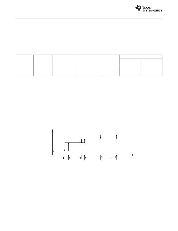
Threshold Voltages
The TPS23757 has a number of internal comparators with hysteresis for stable switching between the various
states. Figure 19 relates the parameters in the Electrical Characteristics section to the PoE states. The mode
labeled Idle between classification and operation implies that the DEN, CLS, and RTN pins are all high
impedance.
PD Powered
Idle
Classification
Detection
V DD -V SS
V CL_H
V CL_ON
V CU_H
V CU_OFF
V UVLO_H
V UVLO_R
Note: Variable names refer to Electrical Characteristic
Table parameters
Figure 19. Threshold Voltages
PoE Startup Sequence
The waveforms of Figure 20 demonstrate detection, classification, and startup from a PSE with type 1 hardware
classification. The key waveforms shown are V VDD -V VSS , V RTN -V VSS , and I PI . This figure shows two detection
cycles (a minimum of two levels are required), a class cycle (a type 2 PSE need only do 1 hardware class cycle if
it reads class 0 through 3), and startup. V RTN to V SS falls as the TPS23757 charges C IN with inrush-limited current
following application of full voltage. Subsequently, the converter starts up, drawing current as seen in the I PI
waveform.
16
Submit Documentation Feedback
Copyright ? 2009–2013, Texas Instruments Incorporated
发布紧急采购,3分钟左右您将得到回复。
相关PDF资料
TPS62230EVM-370
EVAL MODULE FOR TPS62230-370
TRAVELCUBE
SURGE SUP 1OUT W/RJ11 DIRECTPLUG
TRAVELER100BT
SURGE SUP 2OUT W/RJ11 DIRECTPLUG
TRAVELER3USB
SURGE SUPP USB CHARGE TRAVEL SZ
TRAVELERC6
SURGE SUPPRESSOR 120/240V RJ11
TRAVELERC8
SURGE SUPPRESSOR 120/240V RJ11
TRAVELER
SURGE SUP 2OUT W/RJ11 DIRECTPLUG
TRK-MPC5604B
MPC5604B 144PIN REV 2.1
相关代理商/技术参数
TPS23757PW
功能描述:热插拔功率分布 Hi Eff PoE Inter & DC/DC Controller RoHS:否 制造商:Texas Instruments 产品:Controllers & Switches 电流限制: 电源电压-最大:7 V 电源电压-最小:- 0.3 V 工作温度范围: 功率耗散: 安装风格:SMD/SMT 封装 / 箱体:MSOP-8 封装:Tube
TPS23757PWR
功能描述:热插拔功率分布 Hi Eff PoE Interface & DC/DC Controller RoHS:否 制造商:Texas Instruments 产品:Controllers & Switches 电流限制: 电源电压-最大:7 V 电源电压-最小:- 0.3 V 工作温度范围: 功率耗散: 安装风格:SMD/SMT 封装 / 箱体:MSOP-8 封装:Tube
TPS2375D
功能描述:热插拔功率分布 IEEE 802.3af PoE Pwr Device Cntrler RoHS:否 制造商:Texas Instruments 产品:Controllers & Switches 电流限制: 电源电压-最大:7 V 电源电压-最小:- 0.3 V 工作温度范围: 功率耗散: 安装风格:SMD/SMT 封装 / 箱体:MSOP-8 封装:Tube
TPS2375D
制造商:Texas Instruments 功能描述:POWER OVER ETHERNET ((NW))
TPS2375DG4
功能描述:热插拔功率分布 IEEE 802.3af PoE Pwr Device Cntrler RoHS:否 制造商:Texas Instruments 产品:Controllers & Switches 电流限制: 电源电压-最大:7 V 电源电压-最小:- 0.3 V 工作温度范围: 功率耗散: 安装风格:SMD/SMT 封装 / 箱体:MSOP-8 封装:Tube
TPS2375DR
功能描述:热插拔功率分布 IEEE 802.3af PoE Pwr Device Cntrler RoHS:否 制造商:Texas Instruments 产品:Controllers & Switches 电流限制: 电源电压-最大:7 V 电源电压-最小:- 0.3 V 工作温度范围: 功率耗散: 安装风格:SMD/SMT 封装 / 箱体:MSOP-8 封装:Tube
TPS2375DRG4
功能描述:热插拔功率分布 IEEE 802.3af PoE Pwr Device Cntrler RoHS:否 制造商:Texas Instruments 产品:Controllers & Switches 电流限制: 电源电压-最大:7 V 电源电压-最小:- 0.3 V 工作温度范围: 功率耗散: 安装风格:SMD/SMT 封装 / 箱体:MSOP-8 封装:Tube
TPS2375EVM
功能描述:电源管理IC开发工具 TPS2375 POE Powed Device Eval Mod RoHS:否 制造商:Maxim Integrated 产品:Evaluation Kits 类型:Battery Management 工具用于评估:MAX17710GB 输入电压: 输出电压:1.8 V
